| Home | Introduction | Approach
& Model | Computational Process | Calculation of Electric Field | Results & Discussions | References & Appendix |
Introduction:
Carbon nanotubes, made of
only carbon atoms, consist of concentric cylinders of a hexagonal
(graphaitic) network arranged around each other with a helical twist. In a
carbon arc discharge apparatus, bundles of coaxial nanotubes of diameters
ranging between 2 to 20 nm form at the negative electrode. Single-shell
nanotubes of diameters between 1 and 3 nm have also been synthesized by using
metal catalysts and through the plasma decomposition of benzene [Maiti et al.].
To understand the CNTs structure, it helps to imagine
folding a two-dimensional graphene sheet. Depending on the dimensions of the
sheet and how it is folded, several variations of nanotubes can arise. Also,
just like the single or the multilayer nature of graphene sheets, the resulting
tubes may be a single-or a multiwall type. [Meyyappan and Srivastava]
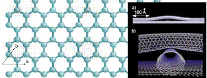
Fig.
1: Two-dimensional sheet of graphene. (Inset: carbon nanotubes- IBM) [Meyyappan and Srivastava]
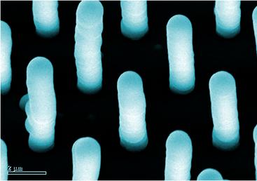
Fig 2:
Array of vertically aligned carbon nanotubes grown using plasma enhanced
chemical vapor deposition is intercalated with SiO2 to provide a bottom-up
process for developing interconnects. These vertical interconnects are ideal
for DRAM applications and three-dimensional architectures. (Source: NASA Carbon
Nanotube Interconnect Image, http://www.ipt.arc.nasa.gov/interconnect2.html)
Carbon nanotubes exhibit extraordinary mechanical properties. For
example, the Young’s modulus is typically over 1 Tera Pascal. Also, the
nanotube along the axis is as stiff as a diamond. The estimated tensile
strength is about 200 Gpa, which is an order of magnitude higher than that of
any other material.
The metallic and semiconducting nature of CNT has given rise to
the possibilities of metal-semiconductor or semiconductor- semiconductor
junctions. These junctions may form nanoelectronic devices based entirely on
single atomic species such as carbon.[ Meyyappan and Srivastava]
Carbon nanotubes (CNTs) have been receiving much
attention for their potential in field emitter devices, displays, sensors,
electrodes and other related applications. Growth on patterned substrates for
these applications is facilitated by chemical vapor deposition (CVD). A DC
plasma through a pair of electrodes is normally added to take advantage of the
electric field effect on alignment. With wide ranging applications for CNTs,
techniques that allow controlled growth on patterned substrates as well as
those for large scale production to meet possible future commodity market needs
(for structural composites) will assume increased importance [Hash et al.]. Thus
an understanding of the CNT growth kinetics is therefore crucial.
The
present work is aimed to develop a finite element analysis (FEA) simulation tool
to facilitate the analytical understanding of the CNT growth. A closed tip CNT
is modeled for 2-D simulations and the effect of different chamber pressures
and voltages on CNT growth rate were discussed. Since dc plasma sources are
widely used now for CNT growth, the present exercise provides useful insight
into the process mechanisms.